- 您现在的位置:买卖IC网 > Sheet目录1992 > DAC7801KPG4 (Texas Instruments)IC DUAL 12BIT CMOS DAC 24-DIP
DAC7800, 7801, 7802
4
SBAS005A
www.ti.com
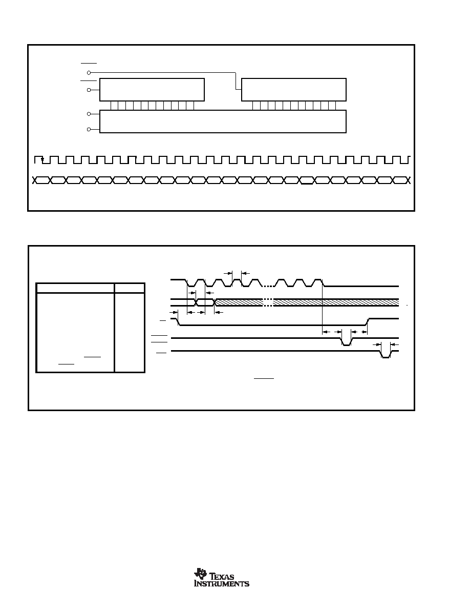
DATA
CS
CLK
t
1
t
5
UPD A
UPD B
t
3
t
7
CLR
t
6
t
8
t
4
0V
5V
0V
NOTES: (1) All input signal rise and fall times are measured from 10% to 90% of +5V. t = t = 5ns.
(2) Timing measurement reference level is V + V
2
F
R
IH
IL
.
t
2
PARAMETER
MINIMUM
t1 — Data Setup Time
15ns
t2 — Data Hold Time
15ns
t3 — Chip Select to CLK,
15ns
Update, Data Setup Time
t4 — Chip Select to CLK,
40ns
Update, Data Hold Time
t5 — CLK Pulse Width
40ns
t6 — Clear Pulse Width
40ns
t7 — Update Pulse Width
40ns
t8 — CLK Edge to UPD A
15ns
or UPD B
TIMING CHARACTERISTICS
VDD = +5V, VREF A = VREF B = +10V, TA = –40°C to +85°C.
Data In
Bit 0
Bit 23
Bit 22
Bit 21
Bit 20
Bit 19
Bit 18
Bit 17
Bit 16
Bit 15
Bit 14
Bit 13
Bit 12
Bit 11
Bit 10
Bit 9
Bit 8
Bit 7
Bit 6
Bit 5
Bit 4
Bit 3
Bit 2
Bit 1
LSB
DAC A
MSB
DAC A
LSB
DAC B
MSB
DAC B
DAC7800 Data Input Sequence
DAC7800 Digital Interface Block Diagram
24-Bit
Shift Register
DAC A Register
UPD A
Data In
CLK
UPD B
LSB
MSB
DAC B Register
LSB
MSB
Bit
23
Bit
12
Bit
11
Bit
0
CLK
DATA INPUT FORMAT
DAC7800 (Cont.)
发布紧急采购,3分钟左右您将得到回复。
相关PDF资料
DAC8043AESZ
IC DAC 12BIT MULT SRL INP 8SOIC
DAC8043GP
IC DAC 12BIT MULTIPLY CMOS 8-DIP
DAC8221GP
IC DAC 12BIT DUAL W/BUFF 24-DIP
DAC8222GPZ
IC DAC 12BIT DUAL W/BUFF 24DIP
DAC8229FSZ-REEL
IC DAC 8BIT DUAL V-OUT 20SOIC
DAC8248FS
IC DAC 12BIT DUAL W/BUFF 24-SOIC
DAC8408GP
IC DAC 8BIT QUAD W/MEMORY 28-DIP
DAC8413EP
IC DAC 12BIT QUAD V-OUT 28-DIP
相关代理商/技术参数
DAC7801KU
功能描述:数模转换器- DAC Dual Monolithic CMOS 12-Bit Multiplying RoHS:否 制造商:Texas Instruments 转换器数量:1 DAC 输出端数量:1 转换速率:2 MSPs 分辨率:16 bit 接口类型:QSPI, SPI, Serial (3-Wire, Microwire) 稳定时间:1 us 最大工作温度:+ 85 C 安装风格:SMD/SMT 封装 / 箱体:SOIC-14 封装:Tube
DAC7801KU/1K
功能描述:数模转换器- DAC Dual Monolithic CMOS 12-Bit Multiplying RoHS:否 制造商:Texas Instruments 转换器数量:1 DAC 输出端数量:1 转换速率:2 MSPs 分辨率:16 bit 接口类型:QSPI, SPI, Serial (3-Wire, Microwire) 稳定时间:1 us 最大工作温度:+ 85 C 安装风格:SMD/SMT 封装 / 箱体:SOIC-14 封装:Tube
DAC7801KU/1KG4
功能描述:数模转换器- DAC Dual Monolithic CMOS 12-Bit Multiplying RoHS:否 制造商:Texas Instruments 转换器数量:1 DAC 输出端数量:1 转换速率:2 MSPs 分辨率:16 bit 接口类型:QSPI, SPI, Serial (3-Wire, Microwire) 稳定时间:1 us 最大工作温度:+ 85 C 安装风格:SMD/SMT 封装 / 箱体:SOIC-14 封装:Tube
DAC7801KUG4
功能描述:数模转换器- DAC Dual Monolithic CMOS 12-Bit Multiplying RoHS:否 制造商:Texas Instruments 转换器数量:1 DAC 输出端数量:1 转换速率:2 MSPs 分辨率:16 bit 接口类型:QSPI, SPI, Serial (3-Wire, Microwire) 稳定时间:1 us 最大工作温度:+ 85 C 安装风格:SMD/SMT 封装 / 箱体:SOIC-14 封装:Tube
DAC7801LP
功能描述:数模转换器- DAC Dual Monolithic CMOS 12-Bit Multiplying RoHS:否 制造商:Texas Instruments 转换器数量:1 DAC 输出端数量:1 转换速率:2 MSPs 分辨率:16 bit 接口类型:QSPI, SPI, Serial (3-Wire, Microwire) 稳定时间:1 us 最大工作温度:+ 85 C 安装风格:SMD/SMT 封装 / 箱体:SOIC-14 封装:Tube
DAC7801LPG4
功能描述:数模转换器- DAC 12B DUAL DAC RoHS:否 制造商:Texas Instruments 转换器数量:1 DAC 输出端数量:1 转换速率:2 MSPs 分辨率:16 bit 接口类型:QSPI, SPI, Serial (3-Wire, Microwire) 稳定时间:1 us 最大工作温度:+ 85 C 安装风格:SMD/SMT 封装 / 箱体:SOIC-14 封装:Tube
DAC7801LU
功能描述:数模转换器- DAC Dual Monolithic CMOS 12-Bit Multiplying RoHS:否 制造商:Texas Instruments 转换器数量:1 DAC 输出端数量:1 转换速率:2 MSPs 分辨率:16 bit 接口类型:QSPI, SPI, Serial (3-Wire, Microwire) 稳定时间:1 us 最大工作温度:+ 85 C 安装风格:SMD/SMT 封装 / 箱体:SOIC-14 封装:Tube
DAC7801LU/1K
功能描述:数模转换器- DAC Dual Monolithic CMOS 12-Bit Multiplying RoHS:否 制造商:Texas Instruments 转换器数量:1 DAC 输出端数量:1 转换速率:2 MSPs 分辨率:16 bit 接口类型:QSPI, SPI, Serial (3-Wire, Microwire) 稳定时间:1 us 最大工作温度:+ 85 C 安装风格:SMD/SMT 封装 / 箱体:SOIC-14 封装:Tube